NEW AMD & Nvidia graphics May Be Doubled With New TSMC Tech
Taiwan Semiconductor Manufacturing Company (TSMC) is boosting the power of graphics cards by Nvidia and AMD. The technology is called wafer-on-wafer, and mimics 3D NAND memory technology used in modern solid-state drives by stacking layers vertically rather than spreading the hardware horizontally across the printed circuit board, which would require additional physical space.
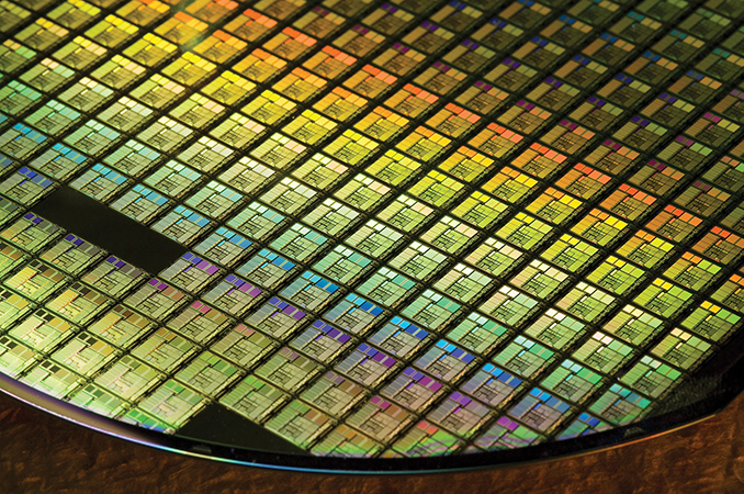
semiconductor_wafer
So what’s a wafer? It’s a thin slice of polished semiconductor material that serves as the foundation for a crisscross of layered copper wires that convey electricity, and the transistors that are the heart of the processor. TSMC introduced its wafer-on-wafer technique during its symposium in Santa Clara, California.
The wafer and mounted components are cut by a diamond saw into single chips and placed into the physical processor package you see when you break open the desktop. The problem with stacking processor wafers may be in the overall manufacturing yields.
The company also revealed a partnership with Cadence for 5nm and 7nm+ process technology for high-performance and advanced mobile computing.
Right now, graphics chips produced by Nvidia and AMD rely on a single wafer. But TSMC, the largest dedicated independent semiconductor foundry on the planet, discovered a way to stack two wafers in a single package. The upper wafer is flipped over onto the lower wafer, and then both are bonded together. Moreover, the upper wafer contains the in/out connection piercings (aka thru-silicon vias), thus the duo is packaged using flip-chip technology.
Tags: AMD, NVDA, gpu, TSMC, AMD & Nvidia graphics, 5nm and 7nm+ process technology,
CONTACTS DETAILS &FOR MORE INFO:
https://www.ultragamerz.com/contact/
- Solana Soars: Could a $450+ SOL Ignite a Meme Coin Frenzy? - June 26, 2024
- Rainbow Six Siege – Official Marketplace Trailer - June 25, 2024
- ImagenAI Poised for Takeoff: Can This Ethereum-Based AI Coin Go 20x? - June 25, 2024